
Blog

Brian Graydon | Nov 4 | 5 min read
The Benefits of Hybrid Microvia Drilling
Updated: Nov 4
The drive for smaller but high-functionality handheld devices led to the implementation of laser-drilled microvias over 20 years ago. Laser drilling of vias is now an established process in the PCB industry for many different circuit applications. Two laser types and three main methods are in use: UV laser drilling only; CO2 laser drilling only; and a combination of both the UV and CO2, commonly referred to as the hybrid process. This hybrid process provides the greatest opportunity for process optimization in the widest range of materials.
The UV laser operates at 355nm and can be used to machine not only copper but also dielectrics (with some caveats mentioned below). The prime use of the CO2 laser (mid-infrared wavelength) is to remove dielectric material, but in certain circumstances it can be used to also punch through copper. Using both lasers in the same machine allows the greatest process versatility to address the wide range of materials in use today.
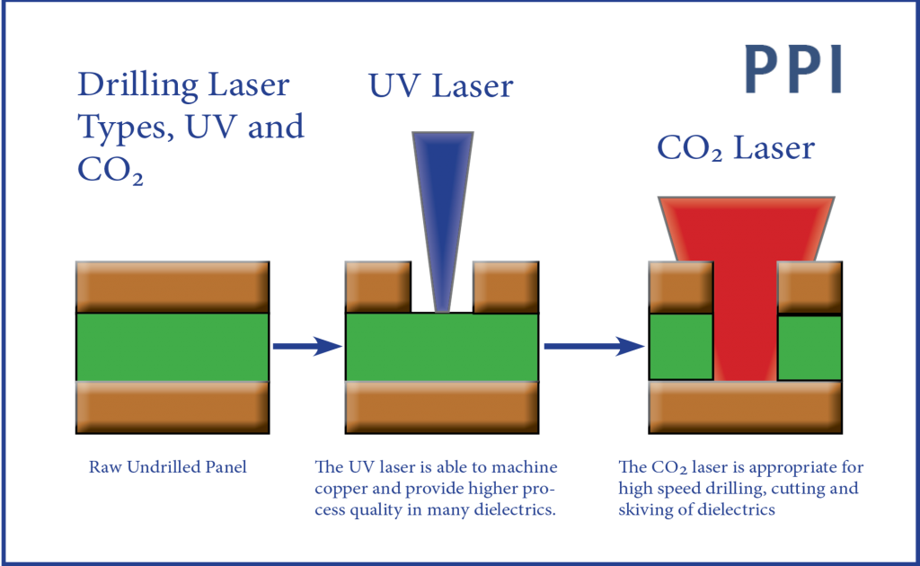
The UV Laser Process
The UV laser is absorbed by both copper and dielectric materials. A high intensity spot is needed to drill through copper while lower intensity is adequate for some dielectrics, notably polyimide and acrylic adhesives used in flexible printed circuits. The high intensity spot can be used to drill through-holes in flex material, while a multi-step process with both high intensity and low intensity process steps can be used to drill blind holes. The laser spot is typically about 20µm in diameter, so for microvias in the 75-150µm diameter range the spot is moved in a spiral pattern to cover the required size. The user-settable laser tool controls the laser repetition rate, pulse energy, hole diameter, and pulse overlap.
If the dielectric is glass-reinforced, as in rigid PCB construction, a UV-only process runs into a problem with blind microvias. The top copper can be machined, of course. However, another high intensity step is needed to remove the glass and epoxy, meaning it will be difficult to remove all the dielectric without also creating damage on the copper stop layer. The process window is very tight, and is not something to be encouraged for production.
The CO2 Laser Process
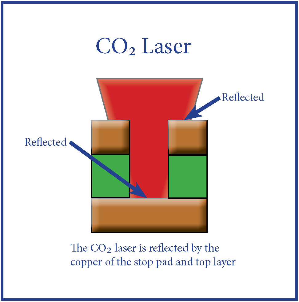
The mid-infrared wavelength of the CO2 laser is strongly absorbed by common dielectric materials and strongly reflected by copper. As a result a large CO2 spot can over-fill an opening in the copper (created by a UV laser or chemically etched) without risk of damage to the top layer of copper surrounding the hole (the capture pad). Repeated pulses will ablate the dielectric (including woven glass reinforcement) and the process self-terminates on the stop layer (target pad) as the beam again is reflected by the copper. A standard desmear has commonly been used for plating preparation.
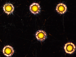
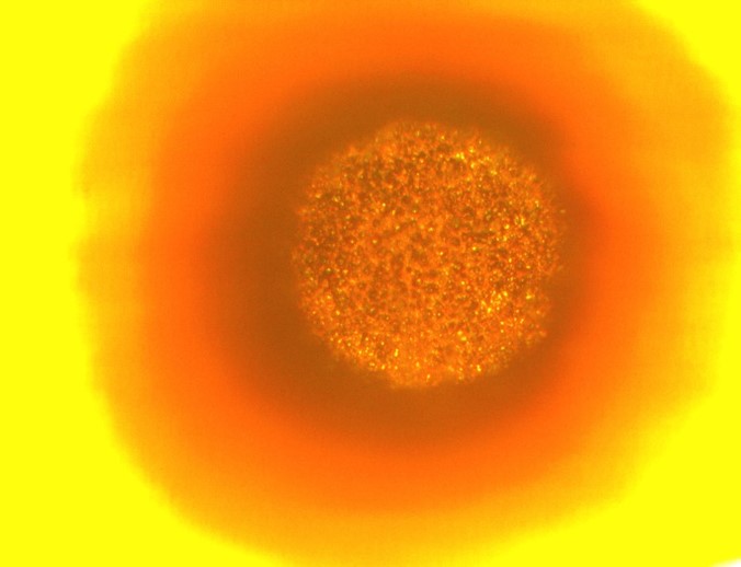
The CO2 spot size is larger than the UV, and a zoom telescope in the ProVia FP-UC models allows any diameter from 80-200µm to be selected. Typically the 200µm spot is used to flood expose vias up to 150µm diameter as shown in the adjacent figure. The laser dose is under user control through the laser repetition rate, pulse length, peak power (which along with the pulse length defines the pulse energy), and number of pulses (in punch mode) or pulse overlap (if spiraling for larger holes).
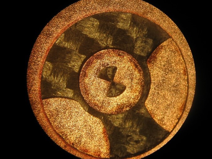
Using the high peak power and smallest standard CO2 spot size in the ProVia of 80µm, there is sufficient intensity to punch through copper up to 9µm thick or more. And with suitable oxide or organic surface treatment on the top copper, holes can be punched in copper up to 18µm thick. Using only two or three pulses to drill through both the copper and a thin dielectric layer will provide a very fast process. This drilling method is employed for high volume production of chip scale packages.
70µm diameter vias punched in Cu (black oxide coating) and dielectric down to the stop pad using only the CO2 laser
The Hybrid Process
Combining both laser sources into one system allows a simple, reliable process with a large process window. The UV laser is used to create the openings in the top copper with high accuracy, etching slightly into the dielectric. This is followed by a CO2 process to remove the dielectric without damage to the top or bottom copper surfaces. Both process steps can be optimized independently to create a very robust production process, one that has been in operation in many PCB shops for over 20 years. The user has complete control over the total energy dose used to remove the copper and then again to drill through the dielectric (pulse energy, number of pulses, peak power, pulse overlap etc.).
The same effect could be generated by drilling first on a UV-only machine and then repeating the job on a CO2-only machine. The drawback here is that panels would need to be moved between machines and then loaded and aligned again for the second process. This problem would be exacerbated if there were 2-layer vias to be drilled anywhere on the panel. A hybrid system with both laser sources would use the one job and perform two passes, the first two-step process (UV followed by CO2) for layer 1-2 and the second two-step process for layer 2-3 drilling, which can also be shifted slightly in focus. The same is true if the user wanted to clean the stop pad (or after skiving to a buried fiducial) with the UV laser; in a hybrid system it’s as simple as adding a third step to the tool used to drill that particular feature.
Buried fiducial exposed after standard UV and CO2 skiving, plus a UV cleaning pass to provide good contrast for the high mag alignment camera
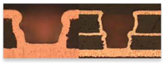
Bottom of microvia after standard hybrid process showing clean but undamaged Cu layer
Single and Two Layer Vias
In summary, a UV system can be used for most flex processing. A CO2-only system can be used for drilling dielectric if openings in the top Cu are pre-etched, or drilling Cu if the Cu is thin and small vias are needed in thin dielectric. To avoid any limitations of one-laser processing the hybrid system (UV and CO2 lasers in one system used in a coordinated fashion) should be used, providing the broadest range of material compatibility (including the latest high speed dielectrics) and widest process window for a robust production process.
Contact PPI about your drilling requirements. Our applications lab is available to process your samples.